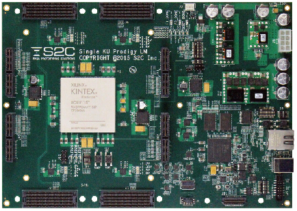
Features and Benefits

Large Capacity & Scalable

  • 1.45M System Logic Cells
  • 75.9 Mb of FPGA internal memory
  • 5,520 DSP Slices
  • Multiple Logic Modules can be conveniently connected together to expand capacity through the use of interconnection modules or cables
  • Up to 16 Single KU Logic Modules can be configured in a Cloud Cube

High Reliability

  • Screw-lock design to high-speed I/O connectors
  • Self-Tests – Isolate design issues from board issues conveniently with a software GUI
  • Monitoring of on-board voltage, current and temperature with a software GUI
  • Automatic shut-down upon detection of overcurrent, over-voltage or over-temperature

Flexible & Powerful I/O

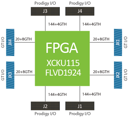
  • 576 high-performance I/O pins and 16 Gigabit transceivers through 4 Prodigy connectors
  • I/O voltage can be adjusted to 1.2V, 1.35V, 1.5V or 1.8V through runtime software in GUI with 4 status LEDs on-board to indicate I/O voltage
  • 32 Gigabit transceivers and 80 GPIOs through 4 GT I/O connectors

High Performance

  • Up to 80W of power for an FPGA
  • Equal trace length for I/Os from same I/O connector
  • 48 Gigabit Transceivers can run at 12.5Gbps

Advanced Clock Management

Standalone Mode

  • 6 global clocks to be selected from
    – 6 programmable clock sources (0.2-700MHz)
    – 5 pairs of external clocks through MMCX connectors
    – 1 OSC socket
  • 3 design clock outputs
    – through 3 pairs of MMCX connectors

Cloud Cube Mode

  • 6 global clocks to be selected from
    – 6 local programmable clock sources (0.2-700MHz)
    – 6 Cloud Cube global clock resources
  • 3 feedback clocks
    – Internally generated clocks can be output to Cloud Cube global clock sources

Ease-of-Use

  • Multiple FPGA configuration options through Ethernet port, USB port, JTAG and micro SD card
  • Auto detection of daughter cards and cables
  • Virtual SWs & LEDs for simple tasks such as changing a setting or indicating a condition remotely
  • User Test Area – LEDs, Push Buttons, Switches and Pin Headers for testing and debugging
  • On-board battery charging circuit makes FPGA bin file encryption easy
  • Optional ProtoBridge™ AXI software to co-model with software/simulation models at the transaction-level
  • Optional S2C design implementation & debug software
  • Compatible with S2C’s off-the-shelf pre-tested daughter boards