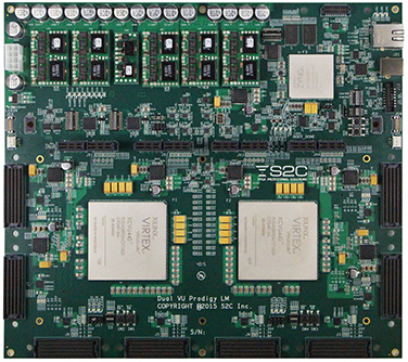
Features
Large Capacity & Scalable
- 11.08M System Logic Cells and 177.2 Mb of internal memory
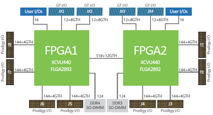
- On-board DDR4 SO-DIMM socket and DDR3 SO-DIMM socket support up to a total of 16GB of memory
- Multiple Logic Modules can be conveniently connected together to expand capacity through interconnection modules or cables
- Up to 16 Dual VU Prodigy Logic Modules can be configured in a Prodigy Cloud Cube
High Reliability
- Screw-lock design to I/O connectors
- Self-Tests – Isolate design issues from board issues conveniently with a software GUI
- Monitoring of on-board voltage, current and temperature with a software GUI
- Automatic shut-down upon detection of over-current, over-voltage or over-temperature
Advanced Clock Management
Standalone Mode
- 6 global clocks to be selected from
– 6 programmable clock sources (0.2-700MHz)
– 5 pairs of external clocks through MMCX connectors
– 1 OSC socket - 3 feedback clock lines for internally generated clocks from any of the two user FPGAs
- 3 design clock outputs
– through 3 pairs of MMCX connectors
Cloud Cube Mode
- 6 global clocks to be selected from
– 6 local programmable clock sources (0.2-700MHz)
– 6 Cloud Cube global clock resources - 3 feedback clocks
– Internally generated clocks in any FPGA can be output to Cloud Cube global clock sources
High Performance
- Up to 100W of power for each FPGA
- Equal trace length for I/Os from same I/O connector
- On-board support of high-speed DDR3 and DDR4 memory
Flexible & Powerful I/Os
- 1,152 general purpose I/O pins and 32 GTH transceivers on 8 Prodigy Connectors
- Prodigy Connector I/O voltage on can be adjusted to 1.2V, 1.35V, 1.5V or 1.8V through runtime software in GUI with 4 status LEDs on-board to indicate I/O voltage
- 32 GTH transceivers and 48 general purpose I/O pins for control signals on 4 GT connectors
Pin-Multiplexing Interconnection Support
- 518 physical interconnections between the 2 FPGAs optimized for pin-multiplexing using LVDS
- Support for 30000+ design interconnections between two FPGAs with LVDS running at 1.2GHz
- Optional Prodigy Player Pro™ Compile Software for automatic design partitioning and LVDS pin-multiplexing insertion
- 12 additional gigabit transceiver interconnections between the two FPGAs
Ease-of-Use
- Auto detection of daughter cards or cables
- On-board battery charging circuit makes FPGA bin file encryption easy
- Compatible with S2C’s off-the-shelf pre-tested daughter boards
- Multiple FPGA configuration options through Ethernet port, USB port, JTAG and micro SD card
- Virtual SWs & LEDs for simple tasks such as changing a setting or indicating a condition remotely
- Optional S2C design implementation software
- Optional S2C Prodigy Multi-Debug System for multi-FPGA deep-trace debug through gigabit transceivers
- Optional ProtoBridge™ AXI software to co-model with software/simulation models in transaction-level

